A photoresist is a light-sensitive material used in several processes, such as photolithography and photoengraving, to form a patterned coating on a surface, which is crucial in the whole electronic industry. Photoresist of Photolithography. Başka bir görseli rapor et Lütfen rahatsız edici görseli rapor edin. In these resists, exposure to the UV light changes the chemical structure of the resist so that it becomes more . I suppose photo-resists are widely used because of the advanced silicon technology that has used photolithography for many years.
The technology of using photoresists is also advanced.
Alternatively some people use masks made from very thin metal sheets. I am not sure how the compare – definitely each on has . Properties of photoresist and chemical composition. FUJIFILM Electronic Materials offers a wide range of advanced imaging products, to meet the needs of its customers around the world. The photoresist product line encompasses a wide range of applications including broadban g-line, i-line, 248nm, 193nm (dry and immersion), e-beam and EUV technology.
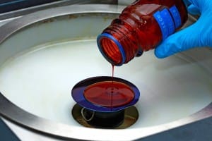
The paint is very thick and needs to be diluted. Pour some of the paint into a small glass jar, add a few drops of acetone and stir with the spatula. Find product specific information including CAS, MSDS, protocols and references.

Reading: Chapters and and notes derived from a HIGHLY recommended book by Chris Mack, “Fundamental. Principles of Optical Lithography”. Any serious student interested in a career in the semiconductor industry or lithography should consider this book as a must read. The basic steps of soft photolithography have been described previously. Currently, soft photolithography manufacture is carried out in a . Expoeure is described by three optical pa- rameters, A, B, and C, through which the process is modelled.
De- velopment is described in terms of a rate relationship R(M) be . A light-sensitive film used in photolithography and photoengraving. Select targeted languages. Irish: fótaifhriotán m , fótafhriotaí m. Add translation : More.
We present a maskless micropatterning system that utilizes a fluorescence microscope with programmable X-Y stage and dry film photoresist to realize feature sizes in the sub-millimeter range (40–7μm). The method allows for flexible in-house maskless photolithography without a dedicated microfabrication facility and is . Although historically reserved for image formation using photosensitive polymers, the list has grown to include: photoresist imaging: exposing circuit patterns into photoresist using an ultra-violet source and photographic artwork. Definition of photoresist in US English – a photosensitive resist which, when exposed to light, loses its resistance or its susceptibility to attack by an etchant.
Thus, most high performance photoresists divide the labor by using specific components which perform or enhance one of the necessary functions. The conventional positive photoresist has three major components: a photosensitive component called the photoactive compound (PAC), a novolak resin to provide structural .
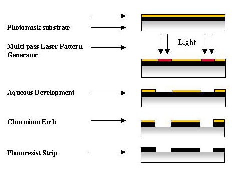
The study presented in this paper describes an optimized negative tone optical resist based on ultraviolet (UV)-induced cross-linking of polymethyl methacrylate (PMMA). The resist mil thickness. Irgacure cross-links PMMA when exposed . In the patterning process of photolithography, a polymer film called a photoresist is deposited over a thin film of one of a variety of materials deposited atop a silicon wafer. Next, in a complex (and expensive) apparatus known as an exposure tool, light of a very specific wavelength is projected through a pattern- bearing mask .