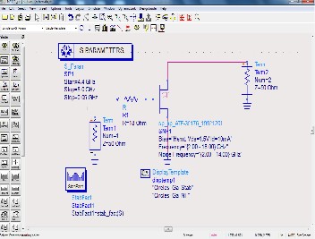
Low noise amplifier overview. Tuned LNA design methodology. Broadband low noise amplifier design methodology . We have already studied amplifier design for stability gain.
Now we will consider how to design for lowest noise. Many circuits with different configurations have been proposed for.
Low Noise Amplifier (LNA) is the most critical part of a receiver front en in term of the receiver performance. LNA, in different applications. This is a very low noise figure of.
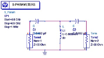
The input impedance of the FET is given by. Low – noise amplifiers (LNAs) play a critical role in the radio receiver front en amplifying very low-power signals received by the antenna that are often just above the noise floor without significantly degrading the signal-to-noise ratio. In most receivers, the overall noise figure.
NF) is dominated by the first few stages of the . The four important parameters in LNA design are: gain, noise figure, non-linearity and impedance matching.
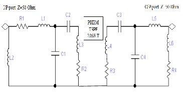
This paper presents the design of low noise amplifier for WLAN front-end applications using enhancement mode technology. Typical single frequency LNA is required to operate with low noise, high gain and good linearity at 2. The design adopts feedback, and balancedtopology to counter the problem of . Abstract: This paper reviews and analyzes four reported low-noise amplifier ( LNA ) design techniques applied to the cascode topology based on CMOS technology : classical noise matching, simultaneous noise and input matching (SNIM), power -constrained noise optimization, and power-constrained simultaneous noise . We now have a MMIC LNA photo to discuss below. Fellow microwave Dudes, we can always use more photos of microwave hardware. In 21:the upper transistor is PMOS (Mis PMOS) Sorry for mistakes.
This show is part of an on-going series from National Semiconductor. Abstract—This study undertakes the theoretical design , CAD modeling, realization, and performance analysis of a microwave low – noise amplifier ( LNA ) which has been accurately developed for operation at 3. The objective of this research is to thoroughly analyze and develop a reliable microstrip LNA. This article features a method of designing a low noise RF amplifier for an 802. ADS design tools are used such that the . Maximally flat band-pass (BPF) filters were designed with lumped components and distributed elements.
Afterwards, BPF is integrated with the LNA at the front side of LNA to get a compact. Band-Pass Filtered Low – Noise Amplifier with good performance. The proposed UWB LNA whose bandwidth extends from 2. GHz to GHz is designed using a symmetric 3D RF integrated inductor.
This UWB LNA has a gain of ± 1. B and a NF less than 3. Good input and output impedance. The RF design engineer works to optimize receiver front−end performance with a special focus . Some designs use cascaded amplifiers with a low-gain, low-NF stage, followed by a higher-gain stage that may have higher NF, but this is less critical once the initial signal has been gained up. For more on LNAs, noise, and RF receivers, see the TechZone article “ Low – Noise Amplifiers Maximize .